
Beyond HBM: How the Memory Wall Could Reshape the Memory Cycle Through 2029
From HBM4 and NVHBM to zHBM, HBC, pooled DRAM, HBF, CMX and software-side memory reduction — the investment question is not which architecture wins, but where durable memory economics survive.
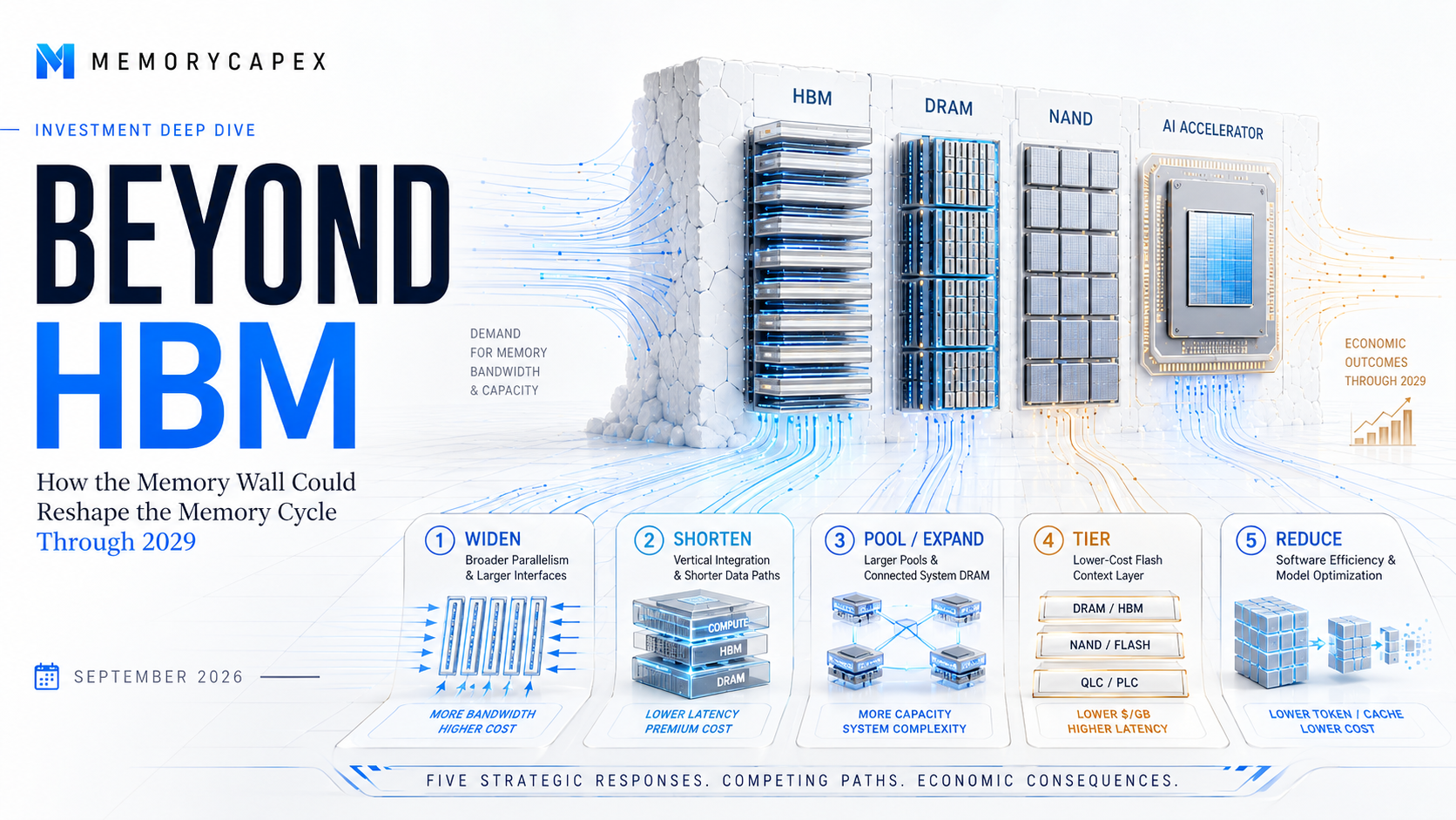
MemoryCapex Investment Deep Dive | September 1, 2026
Executive thesis
The first phase of the AI-memory trade was relatively simple: more accelerators required more HBM, and the suppliers that could qualify and ship HBM at scale captured a disproportionate share of the upside.
That thesis is still valid. It is no longer sufficient.
Inference, longer context windows, retrieval-augmented generation and agentic AI are turning the Memory Wall from a single bandwidth problem into a four-variable constraint: bandwidth, capacity, power and cost per token. The industry is responding with faster local memory, tighter compute-memory integration, larger system-memory pools, flash-based context tiers and increasingly aggressive software techniques that reduce memory demand itself.
Bernstein’s recent memory work captures the broad direction: different AI workloads create different requirements across HBM, conventional DRAM, NAND and storage, widening the opportunity beyond a pure HBM cycle.[1][2] But the investment conclusion cannot stop at “more AI means more memory.”
AI is creating economic pressure for a deeper and more heterogeneous memory hierarchy, but history warns that new intermediate tiers are not automatically durable. Each tier must survive competition from improving adjacent layers and from software that reduces memory demand altogether.
That leads to the central MemoryCapex question for 2026–2029:
Which memory companies can convert AI workload growth into durable pricing power, gross profit per wafer and free cash flow after accounting for substitution, software efficiency, customer architecture and the memory cycle?
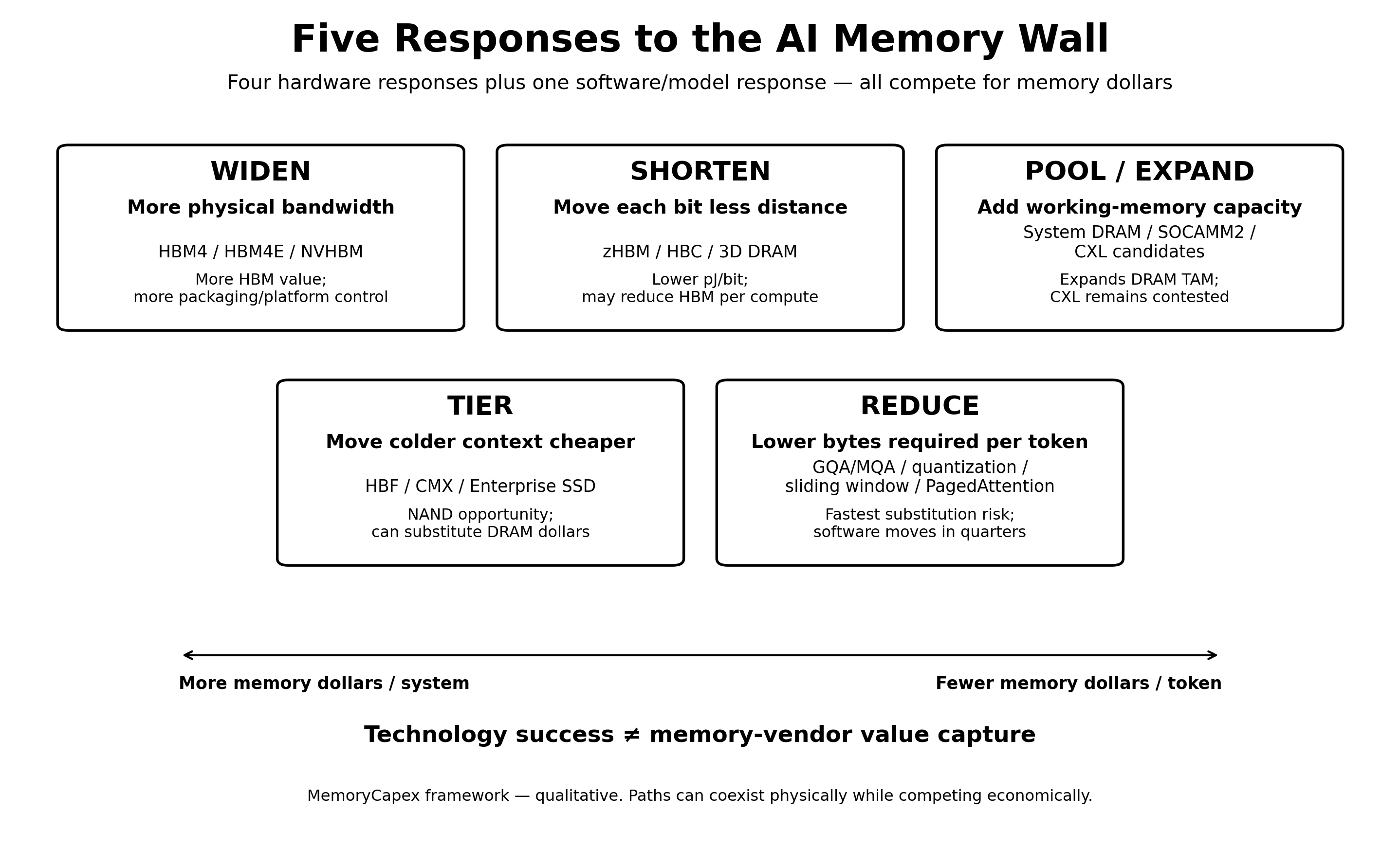
Figure 1. MemoryCapex’s five-path framework. Four paths add or reorganize hardware; Reduce lowers the bytes required per token. The paths can coexist physically while competing economically.
1. Start with the cycle, not the technology roadmap
Any technology thesis in memory is incomplete without locating the industry in the cycle.
The reported economics in mid-2026 are extraordinary. Micron’s fiscal third-quarter revenue reached $41.46 billion. Cloud Memory gross margin was 83%, Core Data Center gross margin 87%, and Mobile & Client gross margin also 87%.[3] The last figure matters: this is not an AI-only upcycle. Pricing power has spread well beyond HBM and data-center products.
SK hynix reported a 76% operating margin in Q2 2026 — a different metric and therefore not directly comparable with Micron’s gross margins — while SanDisk reported an 84.6% gross margin in fiscal Q4 2026.[4][5]
The investor question has therefore changed. We are no longer asking whether memory earnings recover. We are asking how much of today’s scarcity economics survives normalization.
The stock market is already asking that question. In early July, major memory shares entered a technical bear market despite record earnings.[6] SK hynix later reported record absolute results but still disappointed expectations and sold off, a classic late-cycle signal: the marginal stock-price driver can shift from the level of earnings to the direction and breadth of earnings revisions even while reported fundamentals remain excellent.
MemoryCapex’s current-cycle read is late expansion/scarcity, not early recovery. That is not a call that the cycle has peaked. It means the downside mechanism has changed. The key risk is no longer weak demand today; it is future normalization in pricing, supply discipline, memory content per unit of compute, or investor willingness to capitalize unusually high earnings at prior-cycle multiples.
2. The Bernstein paradox: the memory bull case creates its own constraint
Bernstein’s June sector work contains one of the most important contradictions in the current memory thesis.[2]
According to the public summary of the note, conventional DRAM prices had risen roughly 4.5x since Q3 2025, while HBM pricing moved far less because annual contracts locked in earlier pricing. At that point in the cycle, conventional DRAM could generate more than twice the revenue and nearly three times the gross profit per wafer of HBM.
That does not mean suppliers can move committed HBM wafers back to commodity DRAM. HBM qualification, customer commitments, packaging constraints, and strategic relationships limit that response. The better interpretation is an opportunity-cost signal:
Higher conventional-DRAM gross profit per wafer<br> → greater economic cost of allocating scarce DRAM capacity to HBM<br> → stronger supplier pressure in 2027 HBM negotiations<br> → Higher HBM ASPs are needed to restore relative economics.
Bernstein consequently expects HBM pricing to rise sharply in 2027 and placed its 2027 EPS forecasts for Samsung, SK hynix and Micron 25%–38% above the consensus available at the time.[2]
But the same pricing power creates the bear case. Bernstein estimates that rising HBM, conventional DRAM, and NAND could increase the cost of an equivalent AI data-center deployment by up to 30%.[2] This is a modeled incremental capex impact in the public summary — not evidence that memory itself accounts for 30% of the total AI system bill of materials.
The reflexive risk is straightforward:
The more profitable memory becomes, the stronger the incentive for accelerator designers, hyperscalers and model developers to reduce memory dollars per token.
That is why the new architectural paths are not simply a list of bullish memory technologies. Several are customer-funded responses to memory scarcity and cost.
3. What is already expected? Bernstein versus current market consensus
A structural bull case has little investment value if the market already discounts an even stronger outcome.
As of the article lock, analyst-consensus price targets remain highly constructive across much of the sector. Micron’s reference price is $958.73 compared with an average 12-month target of about $1,513. SK hynix’s reference price is KRW 1,653,000 (about $1,203) versus a consensus target near KRW 3,216,025 (about $2,341). Samsung’s reference price is KRW 260,000 (about $189) versus consensus near KRW 471,545 (about $343). SanDisk’s reference price is $1,566.70 versus consensus near $2,125. Kioxia closed at JPY 51,000 (about $319) on September 1 versus consensus near JPY 110,944 (about $694).[15][16][17][18][19]
The U.S.-dollar equivalents use IMF representative rates for September 1, 2026: KRW 1,373.6 per USD and JPY 159.77 per USD.[19]
Bernstein’s published targets are different. Its June targets were $1,300 for Micron, KRW 3,300,000 (about $2,402) for SK Hynix, and KRW 440,000 (about $320) for Samsung.[2] Bernstein maintained a negative view on Kioxia with a JPY 40,000 (about $250) target price, while the broader consensus is strongly positive.[18] Bernstein later raised SanDisk to $3,000.[20]
These are external analyst targets, not MemoryCapex ratings. They are shown only to indicate what may already be discounted in market expectations.
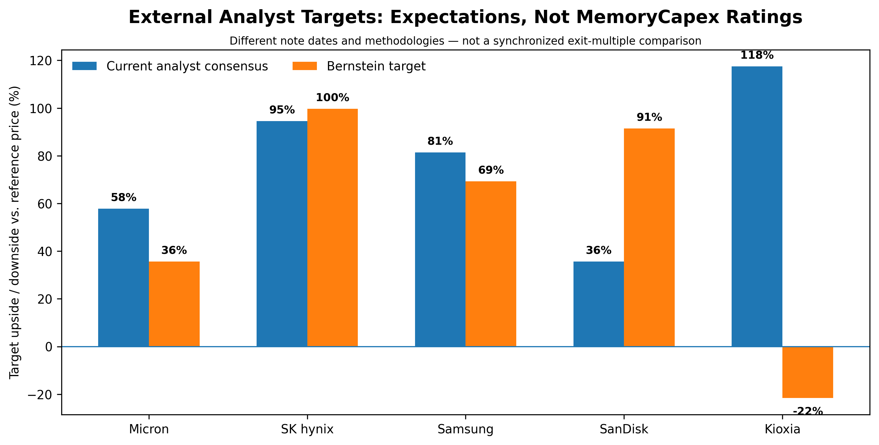
Figure 2. Targets are shown against a common reference price for each stock. Bernstein notes that current consensus estimates are not synchronized in date or methodology; this is an expectations snapshot, not a relative exit-multiple calculation.
A revealing tension appears in Micron. Bernstein’s June 22 target was $1,300 even though its 2027 earnings estimates for the major memory names were 25%–38% above the consensus available at the time. By late August, the broader Micron consensus target had risen to roughly $1,500.
Those observations are not perfectly synchronized, so they should not be used to calculate a precise relative exit multiple. But the direction is still informative: one of the sector’s most aggressive earnings forecasts did not translate into the most aggressive valuation target.
For a late-cycle investor, that is a warning that the debate is shifting from how high earnings can go to what multiple unusually high earnings deserve.
The valuation risk is therefore two-dimensional. Consensus can be wrong about earnings, but the market can also compress the multiple even if earnings remain exceptionally strong. In a cyclical industry, getting the earnings direction right is not enough if investors increasingly treat those earnings as peak-cycle rather than durable.
4. Why inference changes the demand mix — and why KV cache must be derived, not merely cited
Training and prefill remain compute- and bandwidth-intensive. HBM is central because the accelerator needs enormous local bandwidth.
Decode is different. Model weights, and especially the KV cache, are repeatedly accessed. As context length and concurrent users rise, KV cache capacity can become a system constraint.
A simplified decoder-only baseline makes the mechanism visible:
Raw KV bytes ≈ 2 × layers × KV heads × head dimension × cached tokens × bytes per value
Consider a hypothetical 80-layer baseline. This is not a named production model; it is a simplified decoder-only example designed only to show raw memory scale.
- 8 KV heads
- head dimension 128
- 128K active context
- one active sequence
At 16-bit precision, the raw KV cache is approximately 43 GB. FP8 reduces the raw storage to about 21.5 GB. A 4-bit representation reduces it to 10.7 GB, before implementation overhead.
At 32 concurrent full-context sequences, the corresponding raw 16-bit footprint is approximately 1.37 TB before implementation overhead.
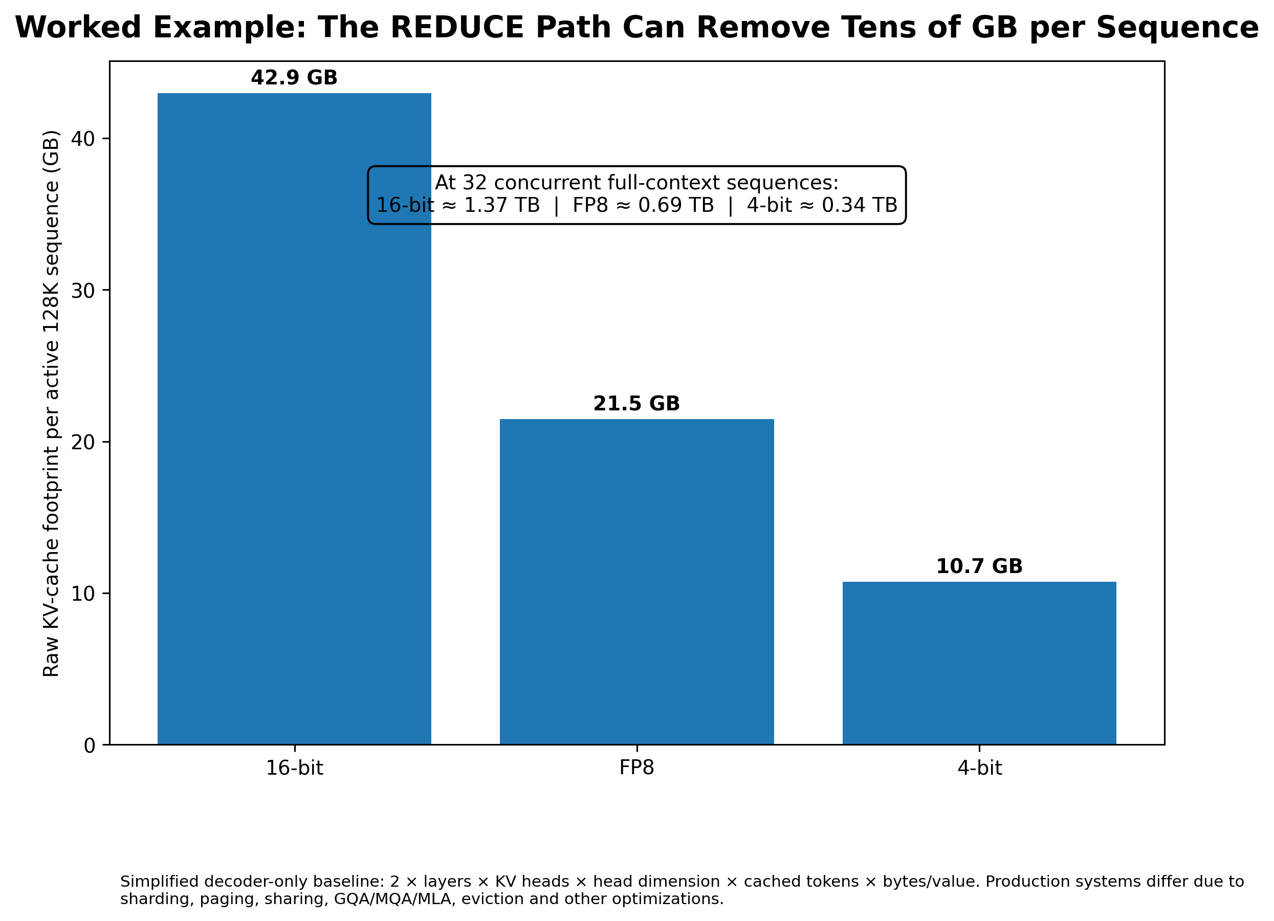
Figure 3. Simplified raw KV footprint. Production systems can differ materially because of sharding, paging, cache sharing, GQA/MQA/MLA, eviction, quantization, and software implementation.
This scaling relationship explains why Bernstein can reasonably argue that KV cache may exceed model-weight memory in large deployments.[1] But whether it does so in a real system depends on architecture, context, concurrency, precision, and cache-management policy.
RAG adds persistent data: vector databases, embeddings and source datasets. Agentic AI adds longer-lived state, tool outputs, and multi-step context.
The economic question is therefore more important than “how much HBM can fit beside the GPU?”
It is:
Which data truly requires HBM, which can sit in system DRAM, which can move into NAND, and how much of that demand can software eliminate before new memory is purchased?
That produces five responses:
Widen / Shorten / Pool-Expand / Tier / Reduce.
5. Widen: HBM4 remains the highest-confidence near-term profit pool
The most direct response to the Memory Wall is more bandwidth besides compute.
The word "widen" is literal. HBM4 doubles the interface width from 1,024 to 2,048 I/O. Micron’s HBM4 combines that wider bus with pin speeds above 11 Gb/s, delivering more than 2.8 TB/s per stack.[7]
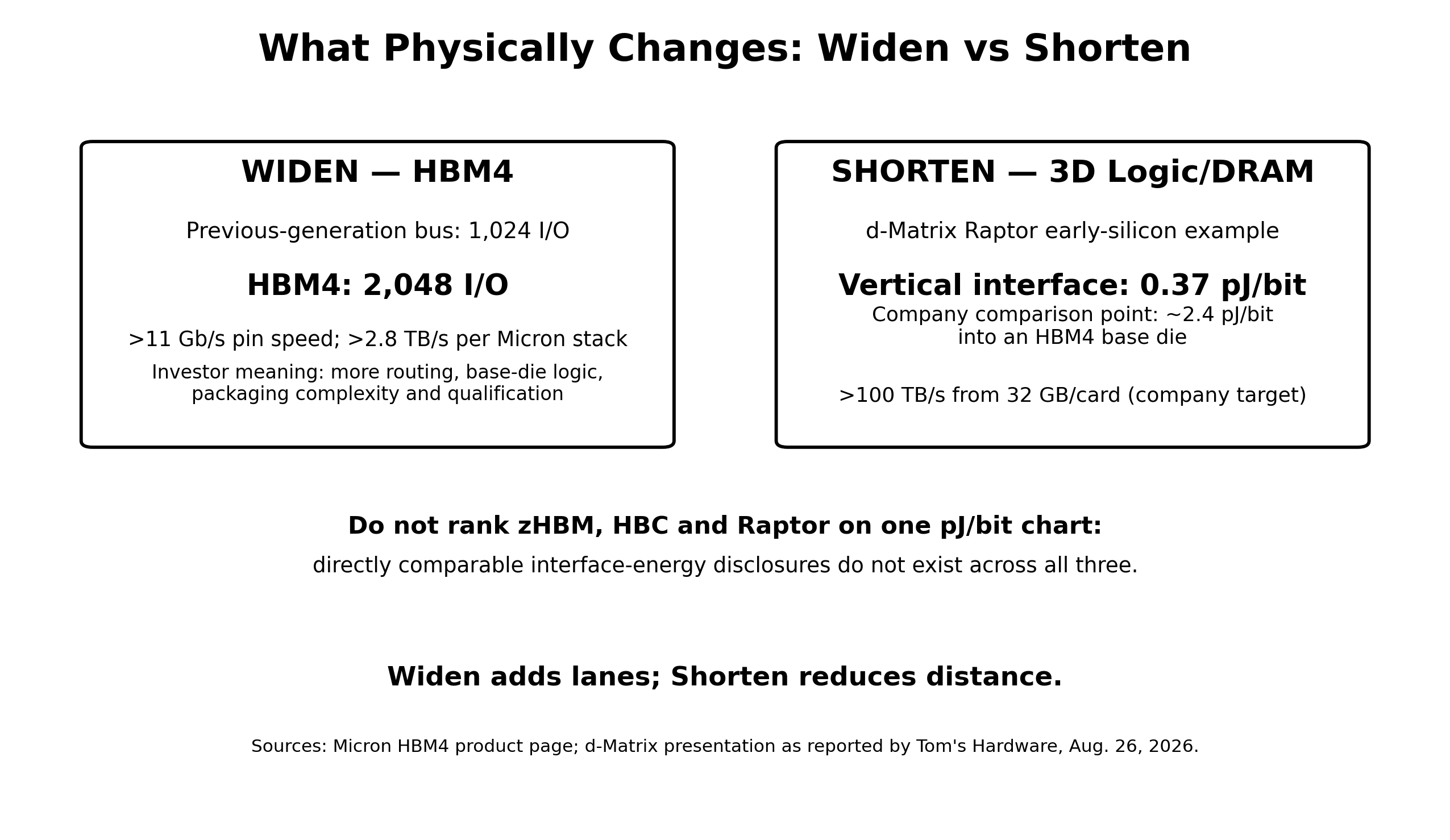
Figure 4. Widen and shorten attack different physical constraints. The d-Matrix energy comparison is a company-reported early-silicon example for early silicon and should not be generalized to zHBM or HBC.
Micron’s 36GB 12-high HBM4 is in high-volume production for NVIDIA Vera Rubin.[7] Samsung began sampling 12-high HBM4E in May 2026 at a stable 14 Gb/s pin speed, scalable to 16 Gb/s, with up to 3.6 TB/s per stack and 48GB capacity.[8] SK hynix began volume HBM4 shipments in Q2.[4]
This is the highest-confidence part of the thesis because it is attached to shipped or sampled products, customer qualification, and visible revenue.
Yet HBM economics are becoming more complex. The relevant metric is not HBM bit growth alone. It is the gross profit per wafer after DRAM opportunity cost, advanced-packaging cost, yield loss, and contract pricing.
In a scarcity cycle, conventional DRAM can temporarily out-earn HBM on a wafer basis. In a normalized cycle, HBM’s structural premium may reassert itself. Investors need to track relative economics rather than assume it.
NVHBM: bandwidth, platform control, and accelerator shoreline
NVIDIA’s NVHBM architecture moves the custom memory controller and PHY into the HBM base die. NVIDIA claims up to 30% more bandwidth per stack, 15% lower HBM power, up to 67% less PHY/support area, and up to 25% more compute-die area for additional XPU capabilities versus standard HBM4E.[9]
The last point matters because NVHBM attacks a less visible scarcity: accelerator shoreline.
Every wide off-die interface consumes finite die-edge routing and PHY area. This is the same physical constraint that weakens some proposals for accelerator-attached CXL. NVIDIA attacks it from the opposite direction: compress the HBM interface footprint and move more memory-interface intelligence into the base die.
For memory suppliers, customization raises engineering complexity and qualification barriers — which is positive for defensibility. But it can also shift bargaining power. If NVIDIA defines the controller, interface, and platform architecture while qualifying multiple memory vendors, more HBM volume does not guarantee that memory suppliers capture the full customization premium.
Custom HBM can raise switching costs while simultaneously shifting part of architectural value capture toward the accelerator-platform owner.
6. Shorten: the physics is data-movement energy
The second response is to move each bit a shorter distance rather than simply moving more bits across a wider interface.
The underlying unit is picojoules per bit (pJ/bit).
At Hot Chips 2026, d-Matrix presented early silicon for its Raptor architecture, which bonds a 4nm compute die face-to-face onto custom DRAM. The company reported 0.37 pJ/bit across the short vertical interface versus roughly 2.4 pJ/bit for moving data into an HBM4 base die in the comparison it presented. Raptor targets more than 100 TB/s from 32GB per card.[21]
Those numbers should not be generalized to Samsung zHBM or Qualcomm HBC because directly comparable pJ/bit disclosures do not exist across all three architectures. But Raptor demonstrates the physical mechanism:
Shortening the data path can reduce the energy tax of moving each bit by multiples — at the cost of capacity, integration complexity and yield risk.
For memory investors, that matters because the profit pool can migrate. If 3D integration materially reduces data-movement energy, value can shift from “more HBM bandwidth” toward bonding, logic-memory co-design, and package-level yield execution.
7. zHBM: when memory becomes part of the accelerator
zHBM deserves more weight than a typical future-product paragraph because it changes where memory sits relative to compute.
Conventional HBM uses 2.5D integration: the GPU or XPU and HBM stacks sit side by side on an interposer. Samsung’s zHBM concept moves toward true 3D integration by stacking HBM vertically above the accelerator, minimizing data-movement distance.[10]
Samsung’s August FMS disclosure described zHBM as a concept model, rather than a commercial product. The company said a next-generation interface incorporating zHBM could deliver approximately 8x the performance of HBM5, more than 10x the memory density, roughly 3x the energy efficiency, and more than a 50% reduction in thermal resistance. Samsung also said customer-specific IP could be integrated into the interlayer between memory and the accelerator.[10]
At SEMICON Taiwan on September 1, industry reporting cited a different comparison baseline — HBM4E — for another set of zHBM system-level targets. Those figures should not be combined with the FMS disclosure in a single quantitative model because the baselines differ and both remain architectural targets rather than measured production specifications.[22]
The strategic implication is Samsung-specific.
Samsung owns DRAM, foundry capability, and advanced packaging. In HBM,4 it already designs a 4nm logic base die internally. If post-HBM5 architecture moves toward deeper 3D logic-memory integration, Samsung’s vertical integration could become more valuable than it is in today’s HBM market.
But integration cuts both ways. zHBM highlights the importance of hybrid copper bonding, wafer bonding, thermal management, customer-specific co-design, and package-level yield. A defect or thermal problem can destroy more value in a more integrated package — a form of yield coupling.
Samsung says first-generation zHBM specifications are still being defined and expects products based on them starting in 2029.[23]
That makes the correct investor hierarchy:
- HBM4: current earnings
- HBM4E: near-term qualification, share and margin battle
- NVHBM / custom HBM: emerging interface architecture and bargaining-power shift
- zHBM: 2029+ strategic optionality with potentially large Samsung-specific consequences
The central uncertainty is not whether zHBM can improve system performance. It is whether Samsung can translate that integration into higher gross profit per accelerator after yield, thermal, and packaging costs.
8. HBC: a direct challenge to the assumption that more AI compute means more HBM
Qualcomm’s High Bandwidth Compute attacks the same data-movement problem from another direction.
Qualcomm describes HBC as a purpose-built near-memory architecture that bonds compute with highly accelerated memory bandwidth in a 3D-stacked silicon solution. Its accelerator roadmap starts from an LPDDR5X-based AI200 platform, and Qualcomm explicitly cites its LPDDR expertise as part of the foundation for HBC.[11]
The key point is that HBC is not simply another HBM generation.
Qualcomm says AI250 with HBC Gen 1 is designed for 133 TB/s of effective memory bandwidth per card, an 18x increase over the AI200, with sampling targeted for mid-2027. Qualcomm also claims a 6x bandwidth-per-watt advantage versus HBM-based solutions when normalized at the card level.[11]
Those figures must not be compared directly with Micron’s 2.8 TB/s per HBM4 stack. HBC is an effective card-level metric; HBM4 is a physical per-stack bandwidth metric.
The investment signal is clearer than the headline number: Qualcomm is explicitly trying to improve inference economics without paying the conventional HBM architecture’s full data-movement cost.
If HBC succeeds, AI workload can grow rapidly while HBM content per unit of compute grows more slowly.
That is the difference between AI growth and memory-revenue growth.
9. Pool / Expand: The requirement is real; CXL is not yet the proven winner
AI systems cannot place unlimited HBM beside every accelerator. Working-memory capacity outside the accelerator must grow.
The strongest current evidence is not CXL. It is system DRAM already shipping. Micron has 192GB SOCAMM2 in high-volume production for Vera Rubin, and SK hynix has also reported growth in SOCAMM2.[7][4]
CXL is one proposed mechanism for expansion, pooling, and disaggregation. The CXL Consortium continues to promote memory tiering, KV-cache offload, and disaggregated memory for AI inference.[12]
But the framework should remain technology-neutral.
SemiAnalysis argued in 2024 that PCIe/CXL faces shoreline-efficiency constraints and that NVIDIA GPUs did not expose CXL in the main AI path.[13] That analysis is now more than two years old and cannot by itself prove the 2026 adoption picture. Nor does promotion by a standards consortium prove commercial deployment.
MemoryCapex therefore defines the path as Pool / Expand, with CXL as one candidate.
The bullish memory point is broader: if inference working sets expand, system DRAM can become a larger part of AI memory content even if CXL never becomes the dominant accelerator-memory fabric.
10. Tier: HBF is a real NAND opportunity — but history says middle tiers often die
High Bandwidth Flash may be the most important new architecture for NAND investors.
SK hynix and SanDisk released the first open HBF specification through OCP in August. The specification supports up to 512GB using 8-high or 16-high NAND stacks and three bandwidth grades ranging from roughly 0.4 to 3.0 TB/s. It also uses UCIe to connect HBF into heterogeneous processor packages.[14]
That means HBF is better understood as a near-compute NAND chiplet tier, rather than a conventional storage device.
But the missing specifications may matter more than the maximum bandwidth.
NAND still has microsecond-class array-read behavior versus nanosecond-class DRAM, and it has finite program/erase endurance. These properties are especially relevant when HBF is used for workloads involving continuous KV-cache updates rather than for largely read-heavy model weights or context.
SanDisk and SK hynix have not disclosed production-level HBF latency or endurance figures.
That silence is investment-relevant.
HBM-class bandwidth should not be interpreted as HBM-class memory behavior.
The success test for HBF is therefore not simply peak bandwidth. It is whether software can hide NAND latency, manage write amplification and endurance, and identify a workload large enough to justify a permanent new tier.
The historical counter-case: intermediate tiers can be squeezed out
The strongest challenge to the “deeper hierarchy” thesis is history.
Intermediate memory technologies can be squeezed from both directions: the fastest tier keeps getting faster while the cheapest tier gets denser and “good enough.”
Intel Optane is the most relevant warning. 3D XPoint was designed to occupy the gap between DRAM and NAND, reached commercial production, and had the backing of a major platform vendor. Intel still ended future Optane development, saying the technology had become impractical to deliver at the required scale as a single-source supplier.[24]
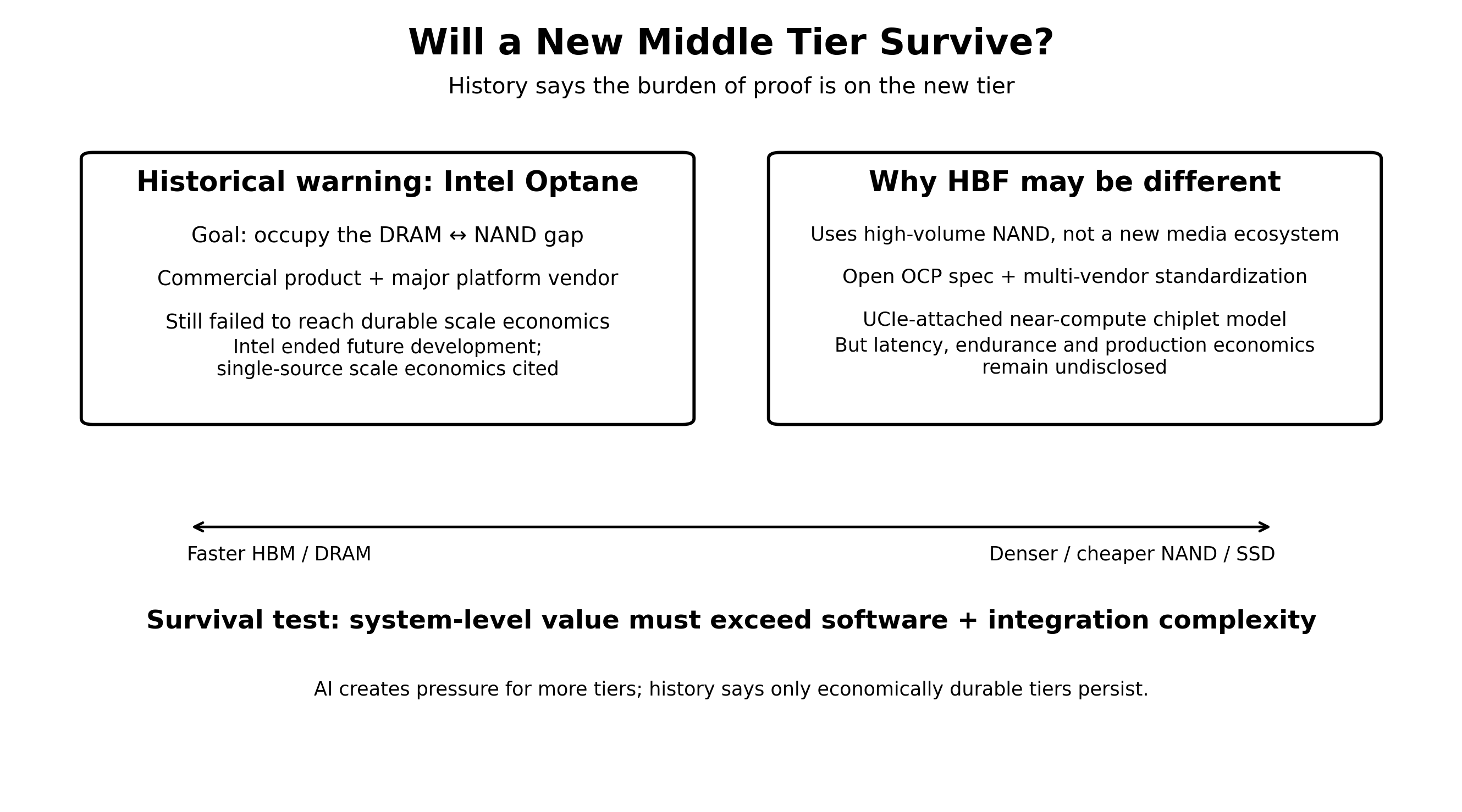
Figure 5. HBF has structural advantages over Optane — it uses conventional NAND economics and an open chiplet-oriented standard — but it still must prove latency, endurance, software and total-system economics.
Why might HBF be different?
Unlike Optane, HBF does not require a novel memory medium or a separate manufacturing ecosystem. It leverages high-volume NAND, open OCP standardization, and UCIe-based chiplet integration.[14]
Those are genuine structural advantages.
They do not guarantee survival.
Google and Tenstorrent's participation in standardization is evidence of ecosystem interest, not proof of production design wins or volume adoption.
The burden of proof is on HBF to show that the incremental system value of a new tier exceeds the software, integration, and operational complexity of maintaining it.
The new falsifier is explicit:
If HBF/CMX remain confined to narrow workloads while improving HBM, system DRAM and conventional enterprise SSDs absorb the same demand, the AI memory stack may polarize rather than deepen.
11. CMX: validation of a context tier, not automatic validation of HBF economics
NVIDIA’s CMX validates the need for a lower-cost context tier.
NVIDIA describes CMX as a flash-based context-memory storage architecture for KV cache and long-context inference. In target workloads, it claims up to 5x tokens per second and 5x power efficiency versus traditional storage approaches.[25]
Those are system-level token and power metrics, not raw memory-bandwidth claims.
For NAND, CMX is structurally positive because it moves flash closer to active inference.
For the memory sector as a whole, it is not automatically positive. If CMX removes expensive context from DRAM/HBM to cheaper NAND, total memory bits can rise while memory dollars and gross profit per accelerator shift downward in the hierarchy.
12. Reduce: the fastest substitution path operates above the silicon
The four hardware paths treat memory pressure as something hardware must accommodate.
That is incomplete.
Model architecture and serving software can reduce the amount of memory required per token before any additional HBM, DRAM, or NAND is purchased.
Examples include:
- GQA / MQA: reduce the number of key/value heads relative to standard multi-head attention; the KV-cache reduction is model-dependent and can be several-fold.
- KV-cache quantization: moving from 16-bit storage to FP8 roughly halves raw storage; moving from FP8 to 4-bit can approximately halve it again, subject to implementation and accuracy trade-offs.
- Sliding-window attention: fixed-window architectures can bound the active cache by the chosen window.
- PagedAttention: reduces fragmentation and redundant duplication and improves throughput by 2–4x at similar latency in the original vLLM work.[26]
- Prefix sharing / eviction / cache policy: improve utilization of installed memory.
NVIDIA notes that FP8 KV cache is already widely used in production and that NVFP4 can reduce the KV cache footprint by about another 50% compared to FP8.[27] Mistral showed that a fixed sliding-window implementation could use a rotating buffer and halve cache memory in its published 8K example.[28]
For memory investors, Reduce is the fastest substitution risk in the framework because software can diffuse in quarters rather than fab cycles.
Any memory-demand forecast that extrapolates KV-cache growth from context length alone is incomplete unless it also models reductions in KV heads, precision, residency, sharing and reuse.
The Jevons counterforce
Efficiency does not automatically mean lower total memory demand.
Lower memory cost per token can be reinvested into:
- longer contexts
- larger batch sizes
- higher concurrency
- richer agentic workflows
- more inference volume
Both forces can operate simultaneously:
Memory intensity per token falls while total memory consumption rises because the number and complexity of tokens expand faster.
The investment variable is therefore not model efficiency in isolation.
It is:
the net change in total memory bytes and memory dollars per unit of deployed compute.
13. Five value regimes: technology success and shareholder success are different things
Memory innovation can create at least five distinct economic outcomes:
<table style="min-width: 100px;"><colgroup><col style="min-width: 25px;"><col style="min-width: 25px;"><col style="min-width: 25px;"><col style="min-width: 25px;"></colgroup><tbody><tr><th colspan="1" rowspan="1"><p>Value regime</p></th><th colspan="1" rowspan="1"><p>Examples</p></th><th colspan="1" rowspan="1"><p>Memory effect</p></th><th colspan="1" rowspan="1"><p>Investor question</p></th></tr><tr><td colspan="1" rowspan="1"><p><strong>More memory dollars</strong></p></td><td colspan="1" rowspan="1"><p>HBM4, HBM4E, SOCAMM2</p></td><td colspan="1" rowspan="1"><p>Mostly incremental</p></td><td colspan="1" rowspan="1"><p>Do ASP and yield support higher gross profit per wafer?</p></td></tr><tr><td colspan="1" rowspan="1"><p><strong>Mix shift</strong></p></td><td colspan="1" rowspan="1"><p>HBF, CMX</p></td><td colspan="1" rowspan="1"><p>More NAND bits; potentially fewer DRAM dollars</p></td><td colspan="1" rowspan="1"><p>Does total memory gross profit rise or merely migrate?</p></td></tr><tr><td colspan="1" rowspan="1"><p><strong>Hardware efficiency</strong></p></td><td colspan="1" rowspan="1"><p>HBC, near-memory compute</p></td><td colspan="1" rowspan="1"><p>Lower data-movement cost</p></td><td colspan="1" rowspan="1"><p>Does memory content per unit of compute fall?</p></td></tr><tr><td colspan="1" rowspan="1"><p><strong>Platform capture</strong></p></td><td colspan="1" rowspan="1"><p>NVHBM, custom HBM</p></td><td colspan="1" rowspan="1"><p>More co-design, more platform control</p></td><td colspan="1" rowspan="1"><p>Who owns the interface economics?</p></td></tr><tr><td colspan="1" rowspan="1"><p><strong>Software substitution</strong></p></td><td colspan="1" rowspan="1"><p>GQA/MQA, KV quantization, PagedAttention</p></td><td colspan="1" rowspan="1"><p>Fewer bytes per token</p></td><td colspan="1" rowspan="1"><p>Does workload growth outrun efficiency gains?</p></td></tr></tbody></table>
A useful simplified framework is:
Memory revenue ≈ workload growth × memory content per system × ASP × product mix
and
Memory gross profit ≈ revenue − wafer/fab cost − advanced-packaging cost − yield penalties.
A technology can increase workload growth while reducing memory content. It can increase the number of bits while shifting the mix from DRAM to NAND. It can raise ASPs until customer elasticity triggers substitution.
This is why gross profit per wafer, gross profit per accelerator, and memory dollars per deployed unit of compute matter more than bit growth alone.
14. Company positioning through 2029
SK hynix — strongest current HBM position, but expectations are already extreme
SK hynix combines HBM leadership with conventional DRAM, SOCAMM2 and NAND exposure through Solidigm, and participates in HBF standardization.[4][14]
The strength is breadth without sacrificing HBM leadership. The principal risk is the other side of that success: very high expectations, large capital requirements, and eventual margin normalization as Samsung and Micron close HBM gaps.
Key metrics: HBM4/HBM4E share, relative gross profit per wafer, capex discipline, SOCAMM2 growth and NAND mix.
SK hynix’s Indiana advanced-packaging facility is scheduled to begin next-generation HBM production in the second half of 2029, creating strategic U.S. capacity but also adding long-duration capital intensity.[29]
Micron — the cleanest observable AI-memory execution, with high cycle sensitivity
Micron now has HBM4, SOCAMM2 and PCIe Gen6 enterprise SSD in high-volume production.[7]
The strength is observable execution across HBM, system DRAM, and storage without relying on distant architecture roadmaps.
The risk is that current margins are exceptionally high and Micron has less publicly visible optionality today in zHBM/HBC-style 3D architectures than Samsung does.
Key metrics: Cloud/Data Center margins, 2027 HBM pricing, SOCAMM2 growth, capex and bit-supply discipline.
Samsung Memory — widest option set; execution determines whether breadth becomes value
Samsung has the broadest architecture portfolio: HBM4/HBM4E, conventional DRAM, NAND, enterprise SSDs, internally designed HBM logic base die, and the zHBM roadmap.[8][10]
Its strategic advantage is vertical integration.
If post-HBM5 architecture shifts toward 3D logic-memory co-integration, Samsung could control more of the value chain than its peers.
But technology breadth is not the same as economic value. Customer qualification, yield progression, base-die execution, and package-level gross profit determine whether breadth translates into market share and cash flow.
SanDisk — the purest listed bet on NAND moving closer to inference
SanDisk has no HBM exposure. Its upside comes from NAND economics and the possibility that HBF upgrades flash from passive storage into an active inference tier.
That optionality matters, but investors should keep the maturity distinction clear: HBF is still in the specification, sampling, and ecosystem formation stages.
The key monitoring items are HBF latency/endurance disclosure, production design wins, enterprise-SSD mix, and whether a new NAND tier earns structurally better gross margins than conventional storage.
Kioxia — the clearest reminder that industry structure and stock valuation are separate questions
Kioxia has strong NAND and enterprise-SSD exposure but no HBM hedge.
Current consensus is strongly positive, while Bernstein’s JPY 40,000 (about $250) target is materially below both the current share price and the consensus.[18]
That divergence is useful because it shows that the same NAND structural thesis can support very different stock conclusions depending on normalized NAND margins, valuation, and the expected duration of current pricing.
HDD — downstream capacity spillover, not the core Memory Wall thesis
Seagate and Western Digital can benefit if AI-generated data becomes a persistent exabyte demand.
But HDD sits far from the active inference path, and the evidence chain is weaker.
For MemoryCapex, HDD should remain a downstream capacity monitor rather than receive the same analytical weight as HBM, DRAM, and NAND.
15. 2026–2029: separate shipped earnings from strategic optionality
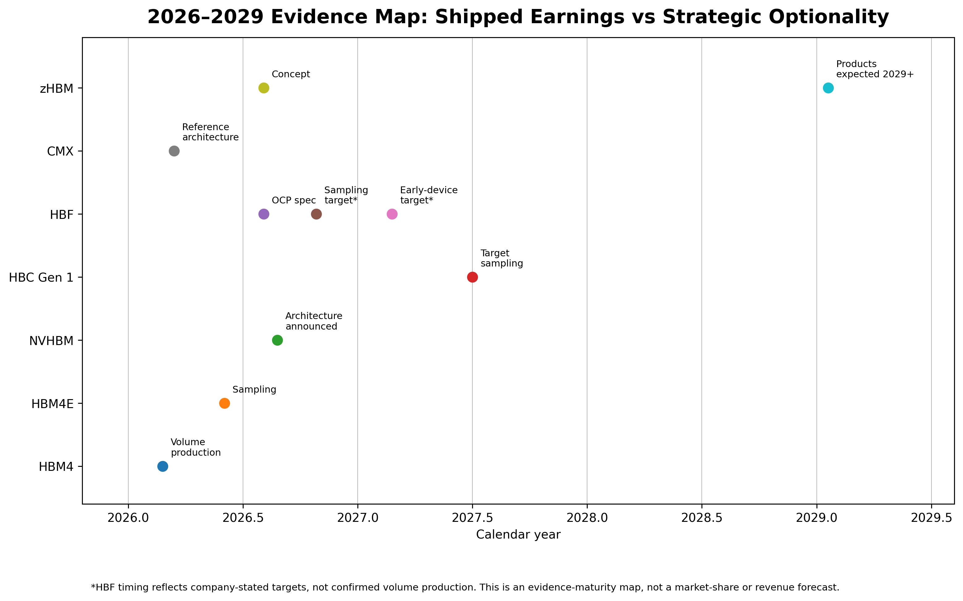
Figure 6. Evidence maturity, not a forecast of market share or revenue.
The investment horizon should be divided into three layers.
2026–2027: scarcity, HBM4 and repricing
HBM4 ramps. HBM4E qualification intensifies. System DRAM expands. 2027 HBM contract pricing becomes a core earnings variable.
This period is driven primarily by supply allocation, yield, contract economics, and customer qualification.
2027–2028: inference-tier experimentation becomes measurable
HBC sampling and HBF/CMX design activity can reveal whether the new architectures are incremental to memory content or substitutional.
The most important questions will be:
- Does HBF disclose competitive latency and endurance?
- Does HBC show real customer adoption?
- Do software-side reductions materially lower memory bytes per session?
- Does system DRAM continue to grow even if CXL remains limited?
2029: architecture begins to matter more than today’s hierarchy
Samsung expects zHBM-derived products from 2029 onward.[23] SK hynix plans next-generation HBM production at its Indiana packaging facility in H2 2029.[29]
By then, the industry may compete as much on 3D integration, base-die logic, customer-specific IP, hybrid bonding, and memory-centric system design as on conventional stack specifications.
But the historical warning remains: not every new tier survives long enough to become a durable profit pool.
16. Scenario framework through 2029
MemoryCapex does not assign precise probabilities because the evidence does not support statistical confidence. The scenarios are ranked qualitatively.
Base case — structurally higher memory value, margins normalize from scarcity peaks
AI workload continues to grow strongly.
HBM4/HBM4E demand remains robust. System DRAM grows with inference. HBF/CMX create incremental NAND demand but remain selective rather than broadly substituting HBM. Software efficiency improves, but context length, concurrency,y and token volume grow fast enough to keep total memory consumption rising.
Supplier capex remains disciplined enough to avoid a severe glut.
Gross margins fall from 2026 extremes but remain above prior-cycle norms.
Bull case — workload growth outruns hardware and software efficiency
AI inference expands faster than memory-efficiency gains.
HBM repricing in 2027 sticks. HBM4E/custom HBM increases dollar content. System DRAM grows sharply. HBF creates a new high-value NAND tier rather than simply cannibalizing DRAM.
Supplier discipline remains unusually strong, and long-term agreements reduce downside cyclicality.
In this case, normalized margins can remain structurally above historical expectations.
Bear case — scarcity economics accelerate substitution and supply response
Memory cost per AI system becomes too high.
Hyperscalers and accelerator vendors are aggressively adopting HBC, HBF/CM, X, and software-side reductions. Memory bytes per active inference session fall faster than context length, concurrency, and inference volume rise.
At the same time, 2027–2029 are arriving faster than demand.
HBM shipments can still rise while gross profit per wafer compresses. NAND bit demand can grow while ASPs and margins normalize sharply.
Excellent technology adoption can coexist with poor stock returns.
A second bear-case path is tier collapse: HBF/CMX fail to earn a durable position because HBM/system DRAM improve above them while conventional NAND/SSD becomes sufficient below them.
17. The MemoryCapex cycle dashboard
The most important metrics to monitor are:
- Gross profit per wafer: HBM vs conventional DRAM. The clearest direct measure of allocation economics.
- Contract pricing: HBM, server DRAM, and enterprise NAND, especially for 2027 negotiations.
- Supplier capex and bit-supply growth: whether scarcity becomes overbuilding.
- HBM qualification and share shifts: SK hynix, Micron and Samsung.
- System DRAM content: SOCAMM2 and server-memory content per AI node.
- NAND in inference: HBF/CMX design wins, shipments, latency/endurance disclosure and enterprise-SSD mix.
- Memory share of AI-system economics: customer response to memory dollars per token.
- Stock/fundamental divergence: whether record earnings still produce negative share-price reactions.
- zHBM milestones: customer engagement, Gen-1 specification, thermal results and packaging yield.
- Consensus revision breadth: whether earnings revisions remain positive or begin narrowing before reported fundamentals weaken.
- Memory intensity per inference session: KV precision, KV-head count, active context retention, prefix-cache hit rate and bytes per concurrent user.
- Tier survival: whether HBF/CMX moves from specification and reference architecture into repeatable production workloads with attractive memory-vendor margins.
MemoryCapex view
The Memory Wall is not an engineering story that later becomes relevant to investors. It is increasingly the mechanism that determines the economics of memory.
Widen can increase memory dollars per accelerator through HBM.
Shortening can improve performance through zHBM, HBC or 3D logic-memory integration, while potentially reducing data movement and memory content per unit of effective compute.
Pool / Expand can broaden AI demand for system DRAM even if CXL itself never becomes dominant.
Tier can create the most important new NAND opportunity in years — but history shows that intermediate memory tiers survive only when their system-level economics justify the complexity.
Reduce can attack memory demand before new silicon is purchased, and it can move faster than any fab cycle.
That makes the next phase of AI memory neither a winner-take-all technology race nor a simple sector-wide bull case.
The competition is for durable value capture.
Today’s scarcity has pushed memory profitability to exceptional levels. That profitability is itself increasing the economic incentive for customers to redesign the stack around lower memory cost per token.
The paradox is central to the cycle:
The more profitable memory becomes, the more economically valuable it becomes for customers to use memory more efficiently.
Through 2029, the strongest memory company will not necessarily be the one with the most bits, the highest peak bandwidth, or the broadest roadmap.
The likely winners will combine:
technology leadership + supply discipline + durable pricing power + control of enough of the architecture to retain the economics after substitution.
For investors, the final question is no longer simply how the Memory Wall will be broken.
It is:
When it is broken, how much of the value created will remain in the income statements and free cash flow of SK hynix, Micron, Samsung Memory, SanDisk and the rest of the memory industry?
Methodology and evidence notes
This article is industry and investment research, not a recommendation to buy or sell any security. Site-wide ownership and conflict-of-interest disclosures apply.
Company technical-performance claims are identified as vendor claims where applicable. Bernstein’s research is used in public summaries because MemoryCapex does not have the full proprietary notes cited here. Third-party analyst ratings and price targets are presented as market-expectation evidence of market expectations, not as MemoryCapex ratings.
The original Widen / Shorten / Extend framing was inspired by the Market Signal video, The Future of AI Memory Is Taking Shape. MemoryCapex expanded the framework into Widen / Shorten / Pool / Tier / Reduce and added the cycle, substitution, tier-survival, and value-capture lenses.
For all non-U.S.-dollar monetary figures, MemoryCapex provides an approximate U.S.-dollar equivalent using contemporaneous exchange rates where relevant.
Sources
- Investing.com, “AI’s memory stack: What investors need to know,” Aug. 29, 2026. <span style="font-size: 12px;">Source</span>
- Investing.com, “Bernstein lifts price targets on memory stocks to reflect higher HBM prices,” June 22, 2026. <span style="font-size: 12px;">Source</span>
- Micron Investor Relations, fiscal Q3 2026 results, June 24, 2026. <span style="font-size: 12px;">Source</span>
- SK hynix Newsroom, Q2 2026 business results, July 29, 2026. <span style="font-size: 12px;">Source</span>
- SanDisk, fiscal Q4 2026 results, Aug. 5, 2026. <span style="font-size: 12px;">Source</span>
- Yahoo Finance, memory stocks enter bear market, July 7, 2026. <span style="font-size: 12px;">Source</span>
- Micron, HBM4 product page and high-volume-production release, Mar. 16, 2026. <span style="font-size: 12px;">Source</span> ; <span style="font-size: 12px;">Source</span>
- Samsung Global Newsroom, HBM4E samples, May 29, 2026. <span style="font-size: 12px;">Source</span>
- NVIDIA Technical Blog, “NVIDIA NVLink Fusion Brings NVHBM to Next-Generation AI Infrastructure,” Aug. 26, 2026. <span style="font-size: 12px;">Source</span>
- Samsung Global Newsroom, zHBM at FMS 2026, Aug. 5, 2026. <span style="font-size: 12px;">Source</span>
- Qualcomm, Dragonfly / High Bandwidth Compute roadmap, June 23, 2026. <span style="font-size: 12px;">Source</span>
- CXL Consortium, FMS 2026 AI-memory use cases. <span style="font-size: 12px;">Source</span>
- SemiAnalysis, “CXL Is Dead In The AI Era,” Mar. 16, 2024. <span style="font-size: 12px;">Source</span>
- SK hynix, “First HBF Standard Specifications with SanDisk,” Aug. 4, 2026. <span style="font-size: 12px;">Source</span>
- Investing.com / MarketScreener, Micron analyst consensus, accessed Sept. 1, 2026. <span style="font-size: 12px;">Source</span>
- Investing.com, SK hynix and Samsung analyst consensus, accessed Sept. 1, 2026. <span style="font-size: 12px;">Source</span> ; <span style="font-size: 12px;">Source</span>
- Investing.com, SanDisk analyst consensus, accessed Sept. 1, 2026. <span style="font-size: 12px;">Source</span>
- Investing.com / S&P Global-derived consensus, Kioxia, accessed Sept. 1, 2026. <span style="font-size: 12px;">Source</span>
- IMF, Representative Exchange Rates, Sept. 1, 2026. <span style="font-size: 12px;">Source</span>
- Investing.com, Bernstein raises SanDisk target to $3,000, June 29, 2026. <span style="font-size: 12px;">Source</span>
- Tom’s Hardware, d-Matrix Raptor Hot Chips 2026 coverage, Aug. 26, 2026. <span style="font-size: 12px;">Source</span>
- EDaily / Korea Times, Samsung zHBM at SEMICON Taiwan, Sept. 1, 2026. <span style="font-size: 12px;">Source</span>
- Yonhap, Samsung U.S. executive on zHBM timeline, Aug. 28, 2026. <span style="font-size: 12px;">Source</span>
- Intel Optane business update. <span style="font-size: 12px;">Source</span>
- NVIDIA Technical Blog, BlueField-4-powered CMX, Mar. 16, 2026. <span style="font-size: 12px;">Source</span>
- Kwon et al., “Efficient Memory Management for Large Language Model Serving with PagedAttention,” arXiv, 2023. <span style="font-size: 12px;">Source</span>
- NVIDIA Technical Blog, “Optimizing Inference for Long Context and Large Batch Sizes with NVFP4 KV Cache,” Dec. 8, 2025. <span style="font-size: 12px;">Source</span>
- Mistral AI, “Mistral 7B,” 2023. <span style="font-size: 12px;">Source</span>
- Reuters / SK hynix, Indiana next-generation HBM production base, Aug. 27–28, 2026. <span style="font-size: 12px;">Source</span>
FX reference used in this article
For non-U.S.-dollar monetary figures, U.S.-dollar equivalents are based on the September 1, 2026 IMF representative exchange rates: KRW 1,373.6 per USD 1 and JPY 159.77 per USD 1. Approximate USD equivalents are rounded for readability.[19]
#HBM #HBM4 #DRAM #NAND #AIMemory #MemoryCycle #MemoryHierarchy #AIInfrastructure #CXL #NVHBM #zHBM #HBF